Zero Point Motion completes Innovate UK project to model first-of-its-kind MEMS-photonics sensor platform
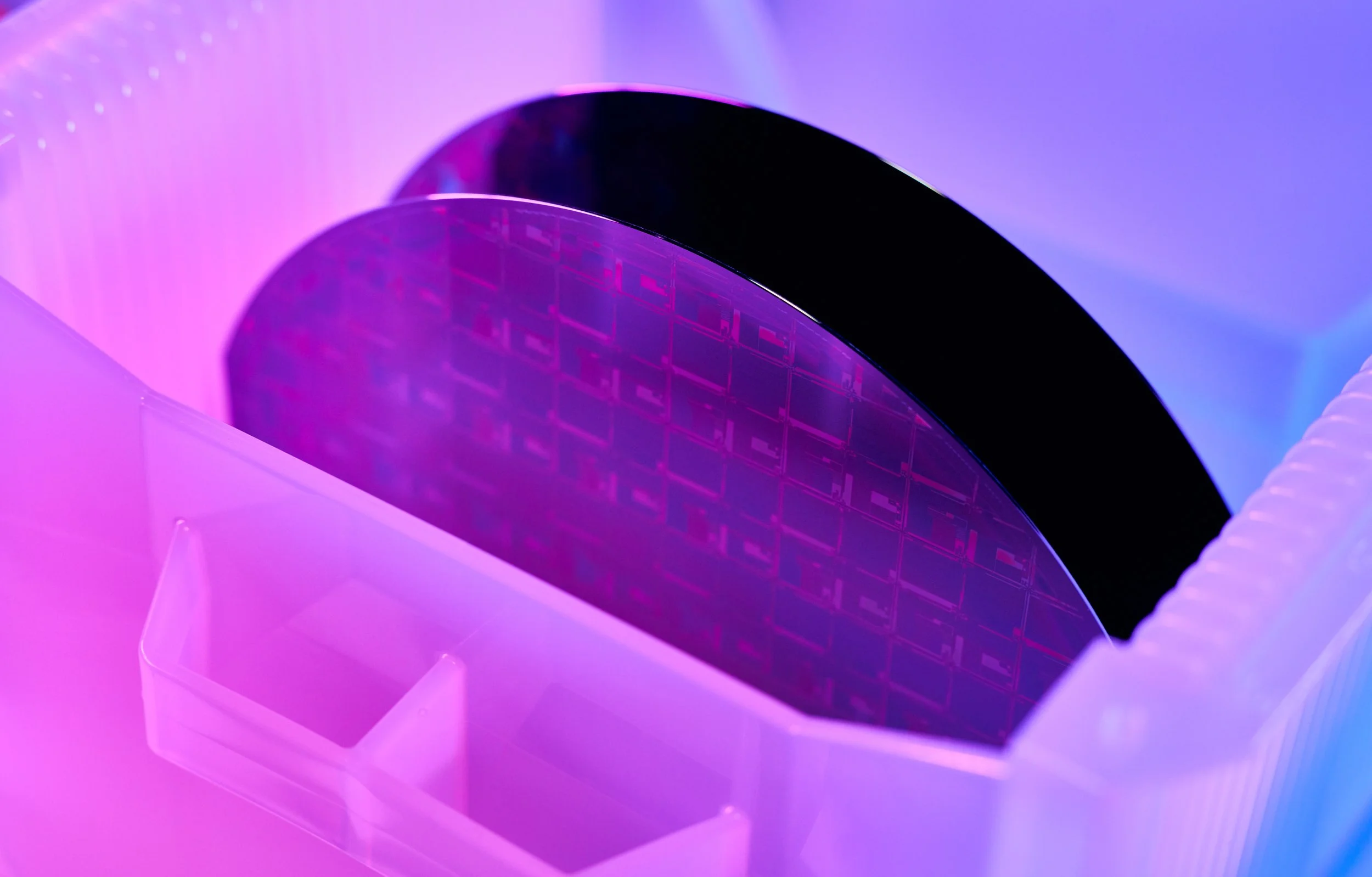
Zero Point Motion in partnership with researchers from University of Bath has successfully completed our latest Innovate UK grant project awarded through the 'Developing Semiconductor Hardware for Critical Technologies' competition. The project, called MIST, stands for Monolithic Integration of Semiconductor Technologies. Its name reflects the core ambition of our technology: creating a first-of-its-kind monolithic platform that combines silicon photonics and MEMS in a single manufacturing stack.
This is a uniquely difficult engineering problem. The MEMS layer in our platform is around 60 µm thick, while the silicon photonics layer is only 220 nm thick, meaning the mechanical layer is more than 270 times thicker than the photonic layer. Bringing these two worlds together requires deep understanding of how materials, etches, undercuts, stresses and wafer-level processes interact after fabrication.
Over the six-month project, we created a new simulation system that can predict how our chips will perform after fabrication, helping us improve our designs faster and reduce risk of errors or delays.
Our team focused on modelling the large differences between etch and undercut behaviour in the very thin silicon photonics layers and the much thicker MEMS layers. Meanwhile, our partners at the University of Bath focused on one of the hardest fabrication effects to predict: wafer bow, where stresses across the wafer can subtly change device geometry and performance after fabrication. While commercial design software was used during the project, the most important parts of the modelling workflow were developed in-house by Zero Point Motion, in collaboration with leading researchers at the University of Bath and informed by real manufacturing data from international semiconductor partners.
This project matters because Zero Point Motion’s MEMS-photonics platform is not only a route to better inertial sensors. We believe it represents a new architecture for sensing itself. By combining the sensitivity of light with the scale of semiconductor manufacturing, the platform has the potential to extend beyond inertial sensing into microphones, ultrasound, pressure, force and other forms of physical perception.
For a monolithic MEMS-photonics platform that does not exist anywhere else in the world, simulation is not simply a design tool. It becomes part of the manufacturing advantage.
Completing this work in just six months required exceptional effort from the team and partners involved. Zero Point Motion is proud of what was achieved in a short period of time, and grateful to Innovate UK, the University of Bath, its contractors and semiconductor partners for helping build a stronger UK capability in next-generation sensor design and manufacturing.
A big thank you to everyone involved in the project.